The Global
Information Hub for
Lighting Technologies
and Design
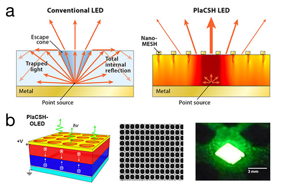
(a) Princeton researchers have used their expertise in nanotechnology to develop an economical new system that markedly increases the brightness, efficiency and clarity of LEDs, which are widely used in smartphones and other electronics. The illustration demonstrates how a conventional LED's structure traps most of the light generated inside the device; the new system, called PlaCSH, guides the light out of the LED. (lllustration courtesy of Stephen Chou et al.) (b) PlaCSH has a layer of light-emitting material about 100 nanometers thick that is placed inside a cavity with one surface made of a thin metal film (shown at left.) The key part of the device is a metal mesh (center) with incredibly small dimensions: it is 15 nanometers thick; and each wire is about 20 nanometers in width and 200 nanometers apart from center to center. An image of the experimental LED is shown at right. (Images courtesy of Stephen Chou et al.)https://zmi.led-professional.com/Plone/media/technology_light-generation_nanotechnology-may-lead-to-better-cheaper-leds_Princeton%20researchers%20have%20used%20their%20expertise%20in%20nanotechnology.jpg/viewhttps://zmi.led-professional.com/Plone/media/technology_light-generation_nanotechnology-may-lead-to-better-cheaper-leds_Princeton%20researchers%20have%20used%20their%20expertise%20in%20nanotechnology.jpg/@@images/image-1200-421696e858fda0c4d328f3ccbd265b07.jpeg
(a) Princeton researchers have used their expertise in nanotechnology to develop an economical new system that markedly increases the brightness, efficiency and clarity of LEDs, which are widely used in smartphones and other electronics. The illustration demonstrates how a conventional LED's structure traps most of the light generated inside the device; the new system, called PlaCSH, guides the light out of the LED. (lllustration courtesy of Stephen Chou et al.) (b) PlaCSH has a layer of light-emitting material about 100 nanometers thick that is placed inside a cavity with one surface made of a thin metal film (shown at left.) The key part of the device is a metal mesh (center) with incredibly small dimensions: it is 15 nanometers thick; and each wire is about 20 nanometers in width and 200 nanometers apart from center to center. An image of the experimental LED is shown at right. (Images courtesy of Stephen Chou et al.)
 Princeton researchers have used their expertise in nanotechnology to develop an economical new system that markedly increases the brightness, efficiency and clarity of LEDs, which are widely used in smartphones and other electronics. The illustration demonstrates how a conventional LED's structure traps most of the light generated inside the device; the new system, called PlaCSH, guides the light out of the LED. (lllustration courtesy of Stephen Chou et al.) (b) PlaCSH has a layer of light-emitting material about 100 nanometers thick that is placed inside a cavity with one surface made of a thin metal film (shown at left.) The key part of the device is a metal mesh (center) with incredibly small dimensions: it is 15 nanometers thick; and each wire is about 20 nanometers in width and 200 nanometers apart from center to center. An image of the experimental LED is shown at right. (Images courtesy of Stephen Chou et al.)")
