The Global
Information Hub for
Lighting Technologies
and Design
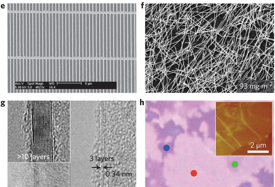
Microstructures of alternative TCE materials: e, Scanning electron microscopy image of a Cu grid with a line width of 200 nm (ref. 41). f, Scanning electron microscopy image of an Ag nanowire network (mass density 93 mg m−2)77. g, Transmission electron microscopy cross-sections of graphene layer stacks (bilayer, triple and multiple layers). h, Optical microscope picture of CVD-grown graphene, transferred to a 300-nm-thick SiO2 layer85. Note the graphene grain sizes of around 10 μm and the ripples (inset) in the graphene layershttps://zmi.led-professional.com/Plone/media/technology_light-generation_new-options-for-transparent-contact-electrodes_Microstructures%20of%20alternative%20TCE%20materials.jpg/viewhttps://zmi.led-professional.com/Plone/media/technology_light-generation_new-options-for-transparent-contact-electrodes_Microstructures%20of%20alternative%20TCE%20materials.jpg/@@images/image-1200-92abc68a4bdb5b4f879107e227f20954.jpeg
Microstructures of alternative TCE materials: e, Scanning electron microscopy image of a Cu grid with a line width of 200 nm (ref. 41). f, Scanning electron microscopy image of an Ag nanowire network (mass density 93 mg m−2)77. g, Transmission electron microscopy cross-sections of graphene layer stacks (bilayer, triple and multiple layers). h, Optical microscope picture of CVD-grown graphene, transferred to a 300-nm-thick SiO2 layer85. Note the graphene grain sizes of around 10 μm and the ripples (inset) in the graphene layers
. f, Scanning electron microscopy image of an Ag nanowire network (mass density 93 mg m−2)77. g, Transmission electron microscopy cross-sections of graphene layer stacks (bilayer, triple and multiple layers). h, Optical microscope picture of CVD-grown graphene, transferred to a 300-nm-thick SiO2 layer85. Note the graphene grain sizes of around 10 μm and the ripples (inset) in the graphene layers")
